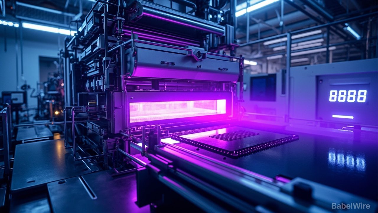
Intel Foundry has reached a major semiconductor manufacturing milestone, processing more than one million 300mm silicon wafers using ASML's High-NA EUV (Extreme Ultraviolet) lithography systems. The achievement is particularly striking because Intel has processed more High-NA EUV wafers than all other chipmakers combined.
The milestone, announced jointly by Intel and ASML, marks rapid progress in High-NA EUV adoption. When ASML shipped its first High-NA EUV tool in late 2024, the industry had barely begun production. By February 2025, only 30,000 wafers had been processed. Reaching one million by September 2026 represents a massive acceleration in cumulative High-NA utilization across the industry.
"With more than one million wafers processed to date, Intel Foundry and ASML are helping customers put High NA EUV to work today," the companies said in a joint press release.
High-NA EUV represents the next generation of semiconductor lithography, with higher numerical aperture enabling finer feature patterning at 8nm resolution with sub-1nm overlay accuracy. The technology is critical for manufacturing chips at the 2nm node and beyond, where conventional EUV lithography reaches its resolution limits.
In parallel with the wafer milestone, ASML and TSMC have announced a separate initiative to accelerate the transition to larger 12-inch (300mm) photomasks for High-NA EUV. The current production standard uses 6-inch (150mm) masks, but the larger format is expected to further reduce per-wafer production costs and increase throughput.
The transition to larger masks is a natural evolution path for EUV lithography. Larger photomasks enable more efficient exposure fields and can reduce the cost per wafer pass — a critical factor as chipmakers push High-NA EUV into higher-volume production across more product lines.
Intel's early and aggressive adoption of High-NA EUV positions it competitively against TSMC and Samsung in the race to produce next-generation chips. Intel 18A, the company's most advanced process node, relies heavily on High-NA EUV patterning for its most critical layers.
The combined announcements underscore a broader trend: the semiconductor industry's most expensive lithography technology is rapidly transitioning from a research curiosity to a production workhorse, with Intel leading adoption and ASML and TSMC collaborating on the next cost-reduction step.