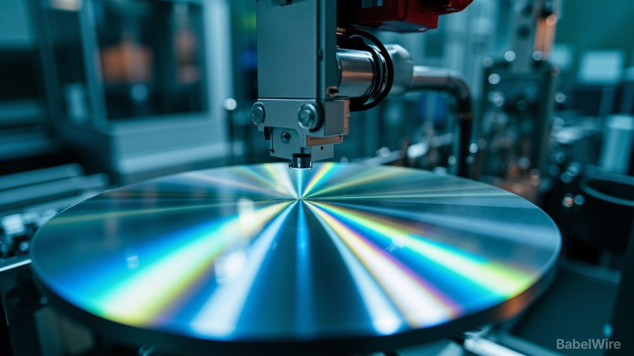
Infineon has processed 300-millimetre silicon-carbide wafers into working power devices at its Villach fab in Austria — the first time functional SiC devices have been produced on the larger format, according to the company. The processed wafer goes on public display at electronica in Munich from 10 November.
The economics are the point. A 300 mm wafer has 2.25 times the area of a 200 mm one, and Infineon puts the gain at roughly 2.3 times as many chips per wafer as it gets today. Crucially, the devices came off equipment built for ordinary silicon, which is what makes the step plausible at industrial scale rather than a laboratory curiosity.
SiC matters because it wastes less power, tolerates higher voltages and temperatures, and carries more current per unit area than silicon. Infineon lists traction inverters, on-board chargers, EV charging infrastructure, grid-scale storage, industrial drives and uninterruptible power supplies as targets — and, increasingly, AI data centres, where SiC is being designed into solid-state transformers, circuit breakers and power supplies for high-voltage DC distribution.
A second piece of the puzzle was demonstrated in Dresden, where Infineon says it has proved its Cold Split wafer-separation process on 300 mm SiC. Cold Split lifts wafers off the crystal instead of sawing them, losing less material per wafer. SiC substrates are the single biggest cost problem in the technology, so anything that yields more wafers from one boule attacks the right number.
What Infineon did not announce matters as much as what it did: no volume ramp date, no wafer-level yield figures, no qualification timeline and no customer shipments. Doubling wafer area does not halve cost per chip — defect density, breakage and usable die yield all have to hold up at the new size, and SiC defects are precisely why the industry stayed at 200 mm.
The milestone sits inside a broader build-out. Infineon's late-October plan to spend about €1.1 billion on 300 mm gallium-nitride production in Villach, targeted for the end of 2027, aims at the same power-conversion market from the high-frequency end. GaN and SiC are complements, not substitutes. The company also continues its 200 mm SiC roadmap.
"With silicon, gallium nitride and now silicon carbide 300-millimetre wafers, we are in a leading position to scale semiconductor manufacturing and drive profitable growth," said chief executive Jochen Hanebeck.
For anyone modelling power-semiconductor supply, the honest reading is this: a manufacturing capability has been shown, not a cost curve. The number to watch next is not wafer diameter but qualified 300 mm die yield, because that is what decides whether this changes prices or only datasheets.
Sources
- infineon.comInfineon press release: world's first 300 mm SiC wafer (electronica 2026)
- electronicsweekly.comElectronics Weekly: Infineon first to fab SiC on 300mm wafers
- convergedigest.comConverge Digest: Infineon produces first 300mm SiC power devices
- golem.deGolem: Infineon 300-mm-SiC-Wafer für leistungsfähige KI-Chips
- semiconductor-today.comSemiconductor Today: first functional power devices on 300mm SiC wafers